Thermal Management Is Addressed in Circuit Board Assembly
The old adage “out of the frying pan into the fire” is more than just an expression of the dangers of moving from one dangerous situation to another; excessive heat can be equally damaging for circuit boards. When a PCB isn’t properly addressed during the assembly process, it can suffer from thermal damage and even fail completely.
Fortunately, this problem can be prevented by proper thermal management. This includes strategic placement of thermal vias that aid heat transfer away from high-power active components. This helps to avoid overheating, which is a leading cause of component and circuit failure.
A circuit board assembly design, layout, and manufacturing processes all play a critical role in thermal management. The design phase involves creating a schematic diagram and specifying the connections for each component. This serves as the blueprint for the layout and component placement. This step also determines the dimensions of traces and spaces for components, which is essential for proper signal flow. Component placement is also critical, as it determines the location of key components for signal integrity and thermal considerations.
How Thermal Management Is Addressed in Circuit Board Assembly
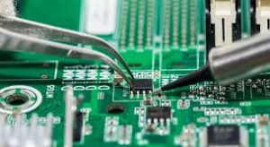
Once the PCB layout is finished, the manufacturing process begins. During this phase, the PCB is placed in a preheat zone to raise its temperature before entering the ramp-up and reflow zones. During these phases, the solder paste is activated by the preheat temperature and melts into place. The components are then inserted into place using a machine that’s capable of picking and placing small parts with high accuracy. Afterwards, the board is inspected and tested to ensure it meets all quality standards.
As more and more components are squeezed into smaller and smaller packages, the amount of heat generated per unit area increases. If this heat isn’t properly dissipated, it can degrade the base laminate, which is made of several layers of raw materials. It can also weaken the solder joints and deteriorate the copper layer, which can reduce the conductivity of the PCB.
This is why it’s so important to consider the needs of a particular circuit board when designing and planning its layout. It’s necessary to size traces and gaps according to the requirements of fast signals, and to choose the right track width, laminate thickness, copper weight or density, and raw material. It’s also vital to ensure the circuit board has sufficient surface area for heat dissipation.
To help with this, it’s recommended to use a wider trace width for high-current circuits and to provide adequate space between each component. This way, the heat produced by each part will spread out more evenly across the surface of the PCB, preventing overheating and reducing the risk of malfunction. In addition to the above-mentioned techniques, there are also other cooling methods that can be used, such as fans, thermal paste, and heat sinks. For the best results, it’s recommended to incorporate a combination of these methods into a circuit board’s design.