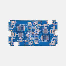
HDI Printed Circuit Boards for High-Speed Applications
When designing high-speed applications, you must carefully optimize every element of your PCB design. This includes choosing the right materials, minimizing power losses and ensuring that all signal paths are as short as possible. This is particularly important when working with HDI circuit boards, which are typically used in more complex electronic devices that demand excellent performance while maximizing space. The best way to do this is by collaborating with an experienced HDI PCB supplier.
Fabricators can optimize hdi printed circuit board for high-speed applications in a number of ways, including using smaller traces and vias, adding more layers, or implementing a stack-up that allows for multiple through holes. In addition, they can utilize different closure technologies to manage heat dissipation. Ultimately, these optimizations must be designed to meet your specific application requirements and the constraints of the manufacturing process.
An experienced supplier can help you select the right materials for your project. They will know which ones are best suited to your unique applications, including their coefficient of thermal expansion (CTE) value, performance under stress, dielectric constant and more. They can also advise you on which fabrication technology is best suited to your product.
How to Optimize HDI Printed Circuit Boards for High-Speed Applications
For example, you might need to work with a manufacturer that offers HDI board technology that supports a particular type of interface, such as the I2C. This is because these boards must be able to communicate with other components within the device at high speeds. In addition, they may need to be able to transmit data across long distances without losing much integrity.
Another consideration when selecting the materials for an HDI circuit board is determining how to accommodate your fabricator’s limitations. This includes determining which material will be best for the manufacturing process and ensuring that it is compatible with the other elements of your circuit board, such as the core substrate, copper plating and component footprints.
The final factor in optimizing your HDI circuit board for high-speed applications is evaluating the layout and construction of your board. This includes analyzing how different via configurations affect density, such as blind/skip vias, staggered and stacked vias, and buried vias. It is also necessary to evaluate the effects of these variables on the overall impedance of your circuit board.
To optimize your HDI PCB for high-speed applications, you should use proper layer stack-up and hole pitching to ensure that the board’s impedance is consistent. This can be achieved by designing a layout that is rational and follows the rules of good PCB engineering, such as avoiding cross-wires and maximizing the use of available space. In addition, you must design your stack-up to minimize heat dissipation, which can be accomplished by utilizing thermal vias and through-hole plating.
You should also consider the use of via-in-pad processes for your HDI PCB, which provide a larger breakout channel for drill wander and reduce the need for via-in-via connections. These techniques can significantly improve the quality of your high-speed signals. Additionally, they can lower the overall power consumption of your device and reduce transmission delays.